Replacing Sony VFETs with lateral MOSFETs
Briefly Sony made semiconductor devices called VFETs. Due to a failure prone device in the iconic TA-4650 amplifier (a double diode called VD-1221M) these transistors would blow up. They can also blow up due to a design flaw in the power supply (D403). Since the VFETs are not manufactured anymore a solution had to be found.
A VFET, or Vertical FET is also known as a SIT (Static Induction Transistor) is a power JFET, or junction FET. This means that it is a depletion type transistor. It conducts when its gate is at zero volts, whereas an enhancement type transistor, usually a MOSFET, is cut off. So, I reckoned, when I use a MOSFET like the IRFP(9)240 HEXFET, I don't need the annoying additional power rail that Sony needed to get its transistors cut off. So I removed it and started testing with these transistors:

It worked beautifully! Only snag is that the thermal stability was crap. After running the amp at high power for a few minutes the bias current would rise to unhealthy levels. This is also very well described in Rod Elliotts excellent article. Not wanting to figure out a second thermal feedback loop (the first one is D302 coupled with Q307) I looked into my MOSFET tray and lo and behold! Found a couple of vintage Hitachi 2SJ161/2SK1057s. This posed a problem. The Vgs threshold of these lateral MOSFETs is close to zero whereas the HEXFETs hover around 4 V. So I had to rebuild the crappy additional power supply. But wait a minute! I don't need al 20 volts of it but only a few. A TL431 regulator with its control pin connected to its cathode regulates to 2.5 V which is perfect to cut off the transistors:

Note that C4 has a value of 10 µF in the final version.
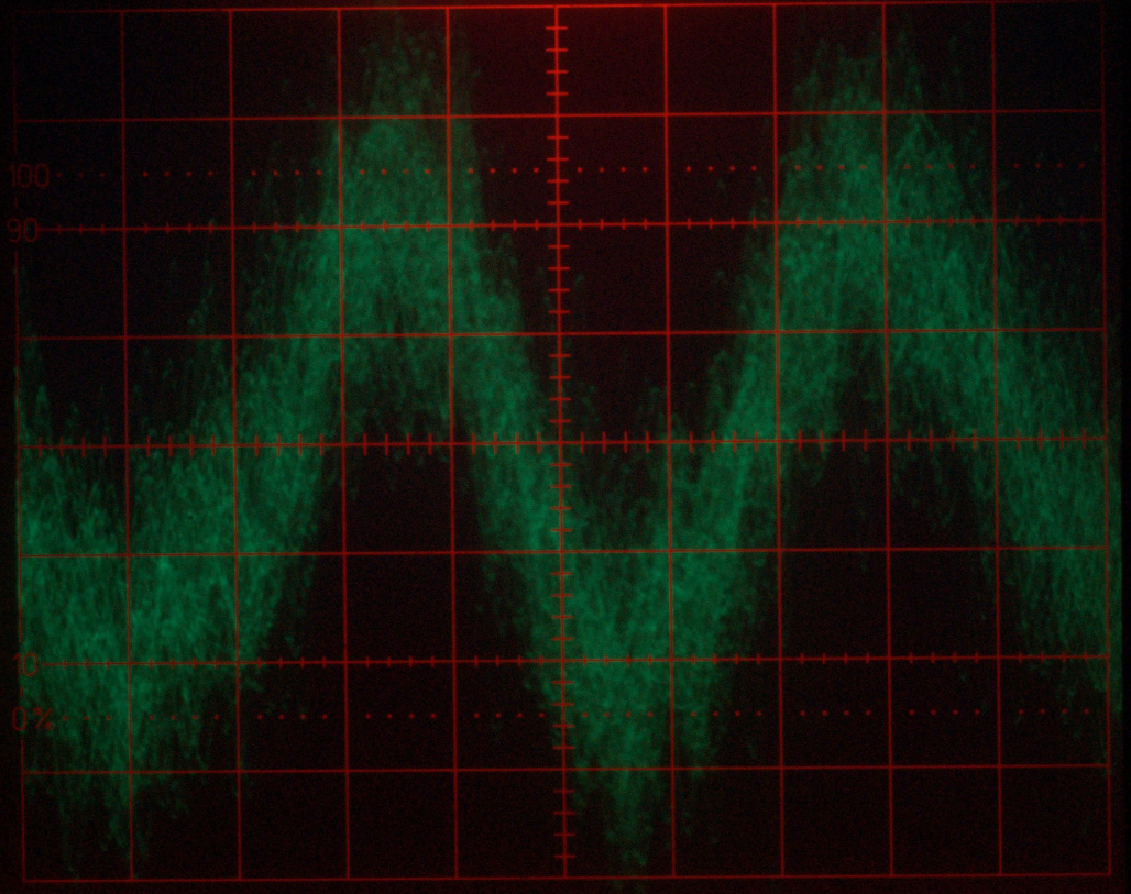
That I really did need it was painfully clear as I hooked a scope on the gate of the 2SJ161:

With the transistor almost cut off it still has enough gain to oscillate. When I put the 2.5 V supplies in the parasitics were gone. But there still was the matter of the biasing. Sony needed a crazy network to mitigate the effects of the supply ripple on the bias current. Also mains voltage variations would upset the biasing. I had gotten rid of it when I removed the second power supply only to find out the biasing became unstable. Fortunately, because it now is stabilized the circuit becomes much simpler:

Getting the compensation network R375/386 right required some trial-and-error but eventually I found the solution above:

No idea why the steps are in the current trace but they coincide with the reversal of the slope of the power supply voltage. The weird parabolic curve is causes by the integrating action of C421.
Eventually I had it all changed to the new design:


And of course the final schematic (click everything to embiggen):

The mod is straigtforward. In any case, replace the double diodes. If you like, replace the semiconductors with new devices, Q301, 306: 2SA733 (general PNP), Q302, 303: 2SA992 (or another low noise PNP), Q305: 2SC945 (KSC945), Q307, 310: MPSA42, Q308, 309: MPSA92 or anything else that will tolerate 200-300 V at 0.5 A. You can also use even beefier transistors for the gate drivers but that is not necessary as these draw only a few mA. The 2.5 V won't let you draw much more anyway because it craps out at 20 mA or so. Once everything is complete, replace the drain resistors of 0.47R with 100R/3W. If anything goes amiss your precious laterals won't fail. Put the bias controls (RT301/351) at their minimal settings (one clockwise, the other anti-clockwise!) and plonk the mains plug in its socket. Do not use a DBT (Dim Bulb Tester) because if the 2.5 V is missing the MOSFETs go full on. Which should be arrested by the drain resistors, but still. Then see if you can dial in a nice bias current. Sony specifies 0.15 A but 50 mA is fine because the MOSFETs are thermally more stable than the VFETs. With R333 and 334 back to their original values check the power delivery. It should be around 50 W (one channel driven). Distortion (provided you can test it) should be 0.01% at 1-2 watts and less than 0.1% before clipping:
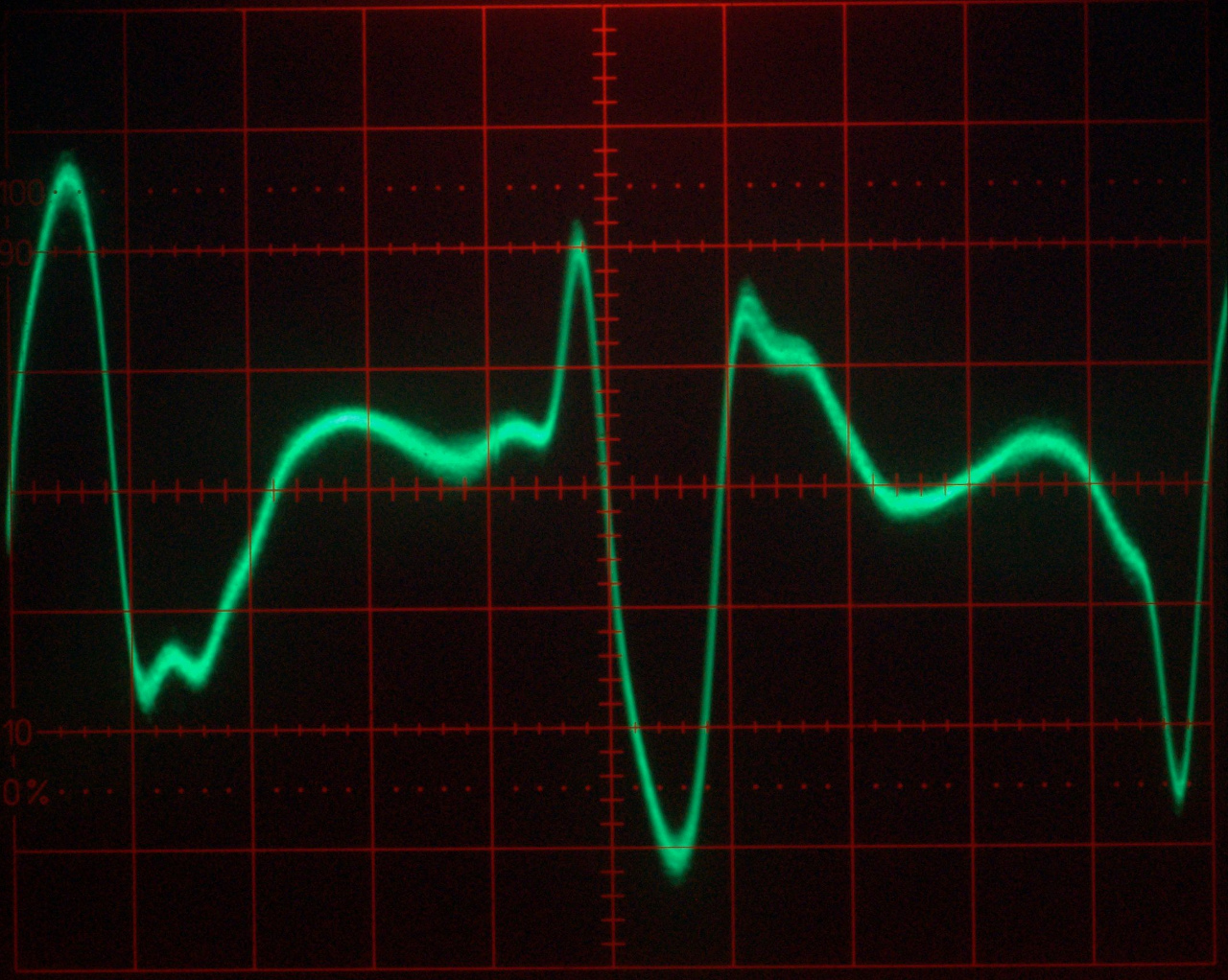
If it is more like in the lower trace (0.4% in this case) this could be caused by bad bias or bad contacts in the plugs on the various boards (amp, psu, relay board). In the case above it was not having proper drive of the laterals (crossover!). The top trace is second order and noise at 0.01%. The traces are from my Lindos LA100 which puts out the distortion component in this test, which is very informative. Clipping is also very noticable but at 1/4 and 3/4 of the trace.
Well, everything was working so it was time for the VFET/MOSFET shootout! As I had both available this was easy:
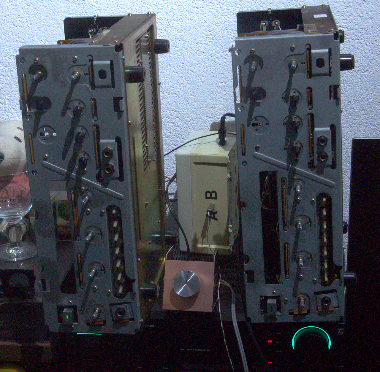
Both amps on top of my trusty DFA888 (REC OUT from a CD). In the middle the level control (Alps RK27/50kA) connected to POWER AMP IN and my speaker toggle box that lets you toggle the speaker so you won't know which amp you listen to. Sort of a poor man's blind test but very effective. The result? After playing many different CDs in many genres I did not hear one iota of difference. These are fine amps, perfectly capable of driving my complex impedance homebrew speakers. And my MOSFET analog turned out to be on par with the VFET original. Mission accomplished! Oh, and in case you want to simulate yourself the LTSpice files are here.
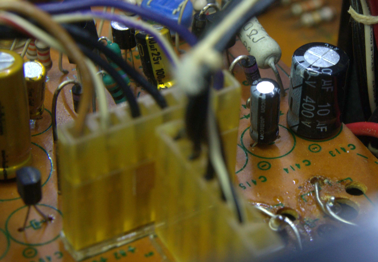
Update: My carefully modded amplifier failed spectacularly due to the failure of C403/413. Apparently electrolytics are unable to cope with the reactive currents going through them. New film caps put things right. Unfortunately they are much bigger than the original electrolytics:


Previous Update: 2 December 2019
Latest Update: 18 September 2025